Linux 7.2 Seeds "Blackwell-Next": A Deep Dive into the nvgrace-gpu VFIO CXL DVSEC Change
- Steve Scargall
- Cxl , Linux
- June 23, 2026
Linux 7.2’s VFIO pull request dropped a commit with a codename I hadn’t seen before: Blackwell-Next. A Phoronix post brought this to my attention - Linux 7.2 Begins Making Preparations For NVIDIA “Blackwell-Next” - which, on the face of it looks like a minor prep patch. It is — but it’s also a clean window into where NVIDIA is taking its CPU-coherent GPU stack, how CXL is quietly becoming the standard signaling interface for next-generation accelerators, and what that means if you’re building infrastructure or tooling on top of these platforms.
Let me walk through what actually changed and what’s interesting about it.
Background: The nvgrace-gpu VFIO Driver
A quick orientation on terms before diving in. VFIO (Virtual Function I/O) is a Linux kernel subsystem that lets a PCIe device be handed directly to a user-space process or VM with full hardware isolation via the IOMMU (Input-Output Memory Management Unit) — the hardware unit that enforces which physical memory a device can DMA to. Think of VFIO as the mechanism that makes GPU passthrough to VMs possible without running a host-side GPU driver. PCIe BARs (Base Address Registers) are the device’s config-space entries that describe memory-mapped regions the device exports to software — every PCIe device has up to six of them. And CXL (Compute Express Link) is the open industry interconnect standard, built on top of PCIe, that adds cache-coherent memory protocols between CPUs and accelerators.
With that context: the nvgrace-gpu driver (drivers/vfio/pci/nvgrace-gpu/main.c) is a VFIO PCI variant driver for NVIDIA’s Grace-based superchips — the GH200 Grace Hopper and GB200/GB300 Grace Blackwell. These are not discrete add-in cards. They’re CPU+GPU superchips where a Grace ARM CPU and one or more NVIDIA GPUs are connected by NVLink-C2C (Chip-to-Chip), a proprietary die-to-die cache-coherent interconnect, with the GPU’s HBM (High Bandwidth Memory — stacked DRAM delivering terabytes per second of bandwidth) directly accessible from the CPU as coherent memory.
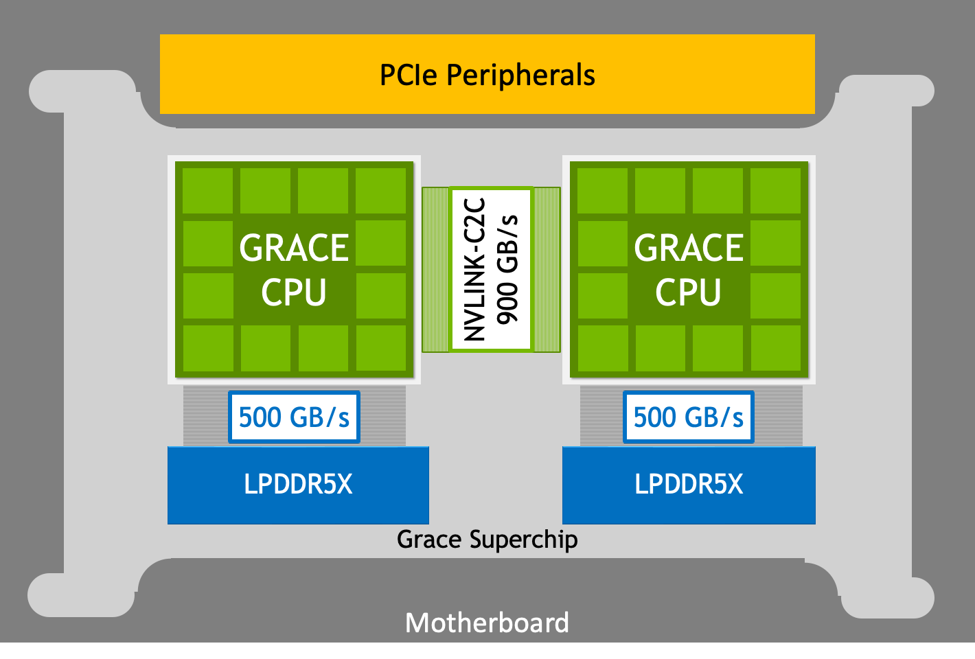
NVIDIA Grace CPU Superchip — two Grace CPUs linked by 900 GB/s NVLink-C2C, the same coherent interconnect topology used between Grace and Hopper/Blackwell GPUs in the GH200 and GB200 superchips. Source: NVIDIA Developer Blog
What this driver does is expose that GPU device memory to KVM (Kernel-based Virtual Machine — Linux’s built-in hypervisor) / QEMU (the open-source machine emulator typically paired with KVM) VMs via VFIO — direct passthrough of coherent GPU RAM to a virtual machine, no host driver interposing on every access. The memory appears to the guest as two 64-bit BARs:
| BAR | Region | Type | Purpose |
|---|---|---|---|
| BAR4/5 | usemem | Cacheable (NORMAL) | Workload GPU memory, GPUDirect RDMA-capable |
| BAR2/3 | resmem | Non-cacheable (NORMAL_NC) | MIG feature support (GH200 only) |
GPUDirect RDMA (Remote Direct Memory Access) is NVIDIA’s technology allowing third-party devices — storage controllers, NICs — to read and write GPU memory directly over the PCIe fabric, bypassing the CPU entirely. MIG (Multi-Instance GPU) is NVIDIA’s GPU partitioning technology that carves a single physical GPU into up to seven isolated instances, each with dedicated memory and compute resources.
The split between usemem and resmem exists because GH200 has a hardware bug: MIG requires a non-cached region, so the driver carves 1 GB off the end of device memory and maps it differently. GB200 and later have the bug fixed — no partition needed, the entire device memory is one cacheable BAR4/5 region.
Memory sizing doesn’t come from the PCI BARs themselves. It comes from ACPI (Advanced Configuration and Power Interface — the firmware/OS interface standard) DSD (Device-Specific Data — a mechanism for attaching vendor-defined key-value properties to a firmware device node) properties that firmware sets:
device_property_read_u64(&pdev->dev, "nvidia,gpu-mem-base-pa", pmemphys);
device_property_read_u64(&pdev->dev, "nvidia,gpu-mem-size",    pmemlength);
Current supported hardware:
| Device | PCI ID | Readiness detection |
|---|---|---|
| GH200 120GB | 0x2342 | BAR0 register poll |
| GH200 480GB | 0x2345 | BAR0 register poll |
| GH200 SKU | 0x2348 | BAR0 register poll |
| GB200 SKU | 0x2941 | BAR0 register poll |
| GB300 SKU | 0x31C2 | probed at runtime (see below) |
That last row is where Linux 7.2 comes in — and it’s also where the “Blackwell-Next” question gets interesting.
What “Blackwell-Next” Actually Changed
The Phoronix article was published 2026-06-21. The commit landed three weeks earlier on 2026-06-02 as 682ecb14e8, authored by Ankit Agrawal (NVIDIA). It touches exactly two files: +163/-12 lines in main.c and +1 line in include/uapi/linux/pci_regs.h.
Worth noting: GB300 (0x31C2) was not added by this commit. That happened 9 months earlier in a separate commit by Tushar Dave (407aa63018, 2025-09-25): “GB300 is NVIDIA’s Grace Blackwell Ultra Superchip.” The Blackwell-Next patch doesn’t touch the device ID table at all.
A Note on What “Blackwell-Next” Means — or Doesn’t
Before going further: “Blackwell-Next” is not an official NVIDIA product name. It appears only in kernel code comments, not in any device ID, capability register, or PCI enumeration table. The commit message says “Add Blackwell-Next GPU readiness check via CXL DVSEC” but never equates Blackwell-Next with a specific PCI ID.
The actual detection in the driver is entirely dynamic. At probe time, the driver calls:
nvdev->cxl_dvsec = pci_find_dvsec_capability(pdev, PCI_VENDOR_ID_CXL,
                                              PCI_DVSEC_CXL_DEVICE);
pci_find_dvsec_capability() scans the device’s PCIe Extended Capability list looking for a DVSEC (Designated Vendor-Specific Extended Capability — a PCIe standard structure, ID 0x23, that lets vendors add custom registers to config space under a registered vendor ID) entry with the CXL vendor ID and device capability type. If found, cxl_dvsec is set to the offset of that capability in config space. If not found, it’s zero.
Every subsequent branch in the driver checks nvdev->cxl_dvsec, not the PCI device ID. Any device registered in the driver’s table that happens to expose a CXL Device DVSEC at probe time will take the CXL readiness path — without the driver needing to know the device ID in advance.
GB300 (Grace Blackwell Ultra, 0x31C2) is the most recent device in the table. Ankit Agrawal — who wrote the Blackwell-Next patch — also reviewed the GB300 device ID commit 9 months earlier. The circumstantial evidence is strong that GB300 is what “Blackwell-Next” refers to. But the code doesn’t state it, and Phoronix, VideoCardz, and WCCFTech all noted the uncertainty when covering this patch.
The Core Problem This Solves
On GH200 and GB200, the driver checks whether the GPU is ready to accept memory access by polling two BAR0 registers: one for HBM training completion and one for NVLink-C2C link status. Both need to read 0xFF before the driver allows VM memory mappings to proceed. This is a proprietary BAR0 register check — those offsets are not defined anywhere outside NVIDIA’s internal hardware spec:
#define C2C_LINK_BAR0_OFFSET     0x1498
#define HBM_TRAINING_BAR0_OFFSET 0x200BC
#define STATUS_READY             0xFF
#define POLL_TIMEOUT_MS          (30 * 1000)  /* 30 seconds */

do {
    if ((ioread32(io + C2C_LINK_BAR0_OFFSET) == STATUS_READY) &&
        (ioread32(io + HBM_TRAINING_BAR0_OFFSET) == STATUS_READY))
        return 0;
    if (schedule_timeout_killable(msecs_to_jiffies(POLL_QUANTUM_MS)))
        return -EINTR;
} while (!time_after(jiffies, timeout));
This requires BAR0 to be mapped during probe: pci_enable_device() → pci_request_selected_regions() → pci_iomap().
On devices where pci_find_dvsec_capability() returns non-zero (i.e., “Blackwell-Next” hardware), the kernel comment says it directly (line 1277):
“On Blackwell-Next systems, memory readiness is determined via the CXL Device DVSEC in PCI config space and does not require BAR0.”
No BAR0 mapping needed at probe time. Readiness signaling has moved into standardized PCIe config space.
The CXL DVSEC Readiness Path
The CXL readiness check reads the RANGE_SIZE_LOW(0) register from the CXL Device DVSEC in config space (offset 0x1C from the DVSEC base, per the CXL specification). Two bits matter:
PCI_DVSEC_CXL_MEM_INFO_VALID(bit 0): device memory information is validPCI_DVSEC_CXL_MEM_ACTIVE(bit 1): device memory is active and accessible
This is straight from CXL spec r4.0 section 8.1.3.8.2, which defines a two-phase readiness sequence:
MEM_INFO_VALIDmust be set within 1 second of reset/power-onMEM_ACTIVEmust be set withinMemory_Active_TimeoutafterMEM_INFO_VALID
That timeout field sits at bits [15:13] of the same register. The encoding is exponential — each step is 4×:
static inline unsigned long cxl_mem_active_timeout_ms(u8 timeout)
{
    return MSEC_PER_SEC << (2 * min_t(u8, timeout, 4));
    /* 000b=1s, 001b=4s, 010b=16s, 011b=64s, 100b+=256s */
}
The worst case is 256 seconds — roughly 8.5× longer than the legacy 30-second BAR0 poll. That’s a meaningful probe-time difference, and it affects more than just probe (see below).
The Locking Challenge
A 256-second wait can’t happen under memory_lock — it would block every VM memory access for the entire duration. The legacy 30-second wait was manageable inside the lock; 256 seconds is not.
The solution is an explicit lockless fast path for CXL devices. In the huge fault handler:
/* Run locklessly before acquiring memory_lock */
if (nvdev->cxl_dvsec && READ_ONCE(nvdev->reset_done) &&
    nvgrace_gpu_wait_device_ready_cxl(nvdev))
    return VM_FAULT_SIGBUS;

scoped_guard(rwsem_read, &vdev->memory_lock) {
    /* Quick re-check under lock to catch reset races */
    rc = nvgrace_gpu_check_device_ready(nvdev);
    if (rc == -EAGAIN)
        goto retry;   /* reset raced the lockless wait — retry, not SIGBUS */
    ...
}
If a device reset races in between the lockless CXL wait and the in-lock recheck, the recheck returns -EAGAIN and the fault handler loops back to the CXL wait rather than returning a spurious VM_FAULT_SIGBUS (bus error signal sent to the VM) to the guest. The same pattern is applied in nvgrace_gpu_read_mem() and nvgrace_gpu_write_mem().
The kernel calls this out explicitly (line 1289):
“Note that the worst-case wait here is ~256s (vs ~30s on the legacy path) and may block device unbind/sysfs for the duration.”
If you’re scripting around this driver and wondering why an unbind is hanging, there’s your answer.
Signal Handling Fix (Both Paths)
The patch also fixed an existing issue on the legacy path. The original msleep() loop was not interruptible — a stuck 30-second probe couldn’t be killed. The patch switches both paths to schedule_timeout_killable(), which returns -EINTR on a fatal signal. No more hung-task kernel panics while waiting on a slow device.
As Alex Williamson summarized in his VFIO pull request to Linus for Linux 7.2:
“Add CXL DVSEC-based readiness polling for Blackwell-Next in the nvgrace-gpu vfio-pci variant driver, including interruptible, lockless waits to support worst case spec defined timeouts. (Ankit Agrawal)”
Is This Driver Actually Useful Today?
Yes. This is not a placeholder or an early stub. The nvgrace-gpu driver has been production-grade since GH200 launched in 2023-2024. The “Supported” status is in the Linux MAINTAINERS file, copyright 2024 NVIDIA. GH200 systems are deployed at scale in AI data centers and research labs. GB200 is shipping to enterprises and hyperscalers now.
The GB300 device ID (0x31C2) has been in the table since September 2025. This Blackwell-Next patch adds the readiness path for devices that use CXL DVSEC signaling. Without it, any such device in the table would fall through to the legacy BAR0 poll — on hardware that doesn’t expose readiness through BAR0 registers — and either timeout or behave unpredictably.
Standard KVM/QEMU needs no modifications. The VFIO character device interface is unchanged. No new sysfs attributes. No new devdax nodes. The VM guest sees the same BAR layout it always has. The only behavioral changes from the VM operator’s perspective are: longer probe wait (up to 256s for CXL-capable devices) and interruptible probes (previously stuck if slow).
What the P2P TODO Tells Us
There’s a commented-out block in nvgrace_get_dmabuf_phys() that’s worth reading:
/*
 * if (nvdev->resmem.memlength && region_index == RESMEM_REGION_INDEX) {
 *     The P2P properties of the non-BAR memory is the same as the
 *     BAR memory, so just use the provider for index 0. Someday
 *     when CXL gets P2P support we could create CXLish providers
 *     for the non-BAR memory.
 * }
 */
P2P DMA (Peer-to-Peer Direct Memory Access — direct transfers between two PCIe devices, such as GPU ↔ NIC, without involving the CPU or system RAM) via GPUDirect RDMA works today through the BAR0 P2P provider for both memory regions. The comment is noting that once the CXL subsystem gains native P2P DMA support, the non-BAR memory could have CXL-specific providers instead. That’s a future optimization, not a missing feature. Device-to-device DMA works today.
For CXL Software Architects
Linux 7.1 landed the CXL Type 2 accelerator infrastructure — exporting internal structs so external drivers can bind Type 2 devices (accelerators with attached memory, rather than pure memory expanders) into the CXL stack:
/* 7.1: cxl: export internal structs for external Type2 drivers */
/* 7.1: cxl: support Type2 when initializing cxl_dev_state */
Linux 7.2 (this patch) moves GPU readiness signaling onto the standardized CXL DVSEC mechanism. These two releases are not coincidental — they represent NVIDIA progressively aligning the Grace GPU stack with CXL protocol semantics rather than proprietary register conventions.
If you’re building accelerator management tooling on top of nvgrace-gpu, the cxl_dvsec field in nvgrace_gpu_pci_core_device is now the detection signal for device generation. Zero means legacy (GH200/GB200 with BAR0 readiness); non-zero means the device uses CXL DVSEC signaling. The nvgrace_gpu_wait_device_ready_cxl() function implements the spec-defined state machine against pci_regs.h constants — no vendor-specific register knowledge required. The PCI_DVSEC_CXL_MEM_ACTIVE_TIMEOUT macro, added to include/uapi/linux/pci_regs.h by this commit, is now part of the stable uapi header set.
What hasn’t changed: no new sysfs entries, no new devdax (/dev/daxN) nodes, no changes to ACPI DSD property names, and no VFIO ioctl changes. If your tooling reads nvidia,gpu-mem-base-pa or nvidia,gpu-mem-size from ACPI, that interface is unchanged. If it drives VFIO read/write/mmap operations, those are unchanged. The only thing that changed is how long probe might take and whether it can be signaled.
Speculating on Vera Rubin
This is where I shift from “what the code says” to “what I think it means,” so take it with a pinch of salt.
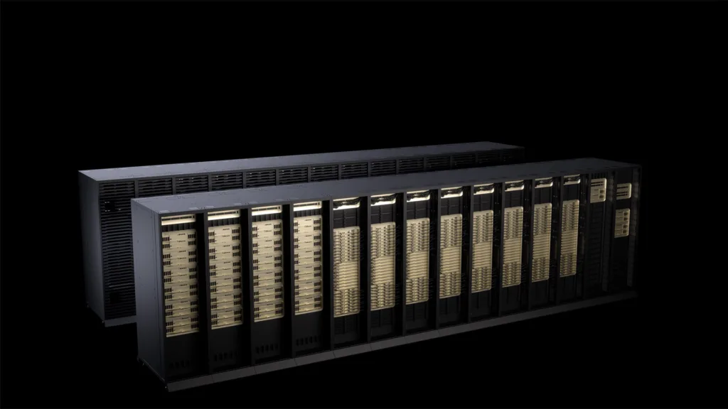
The NVIDIA Vera Rubin NVL72 rack system, announced at CES 2026. Vera CPU supports PCIe Gen6 and CXL 3.1 — the first NVIDIA CPU to list CXL. Source: NVIDIA Developer Blog
NVIDIA’s Grace CPU (paired with Hopper and Blackwell GPUs) supports PCIe Gen5. The Vera CPU — paired with Rubin GPUs in the next-generation superchip arriving H2 2026 — explicitly supports PCIe Gen6 and CXL 3.1. That’s the first time NVIDIA has listed CXL on a CPU specification. NVLink-C2C Gen2 doubles coherent bandwidth from 900 GB/s to 1.8 TB/s and connects Vera to two Rubin GPUs per superchip, with up to 288 GB HBM4 per GPU.
RAS (Reliability, Availability, Serviceability — error detection, logging, and recovery infrastructure in server-class hardware) and memory coherency across these larger HBM stacks is exactly where the CXL DVSEC readiness contract matters. The Memory_Active_Timeout field encoding up to 256 seconds wasn’t written for small devices — it reflects that HBM4 initialization at 288 GB/GPU density genuinely takes more time than what a 30-second proprietary BAR0 poll could safely cover.
The pattern this commit establishes is significant: pci_find_dvsec_capability(pdev, PCI_VENDOR_ID_CXL, PCI_DVSEC_CXL_DEVICE) at probe time, followed by a clean branch to the CXL DVSEC state machine. A future Vera+Rubin VFIO variant driver would use the same pattern — except there would be no legacy BAR0 fallback. The CXL DVSEC path would be the only path, with Grace’s proprietary register offsets obsolete.
The P2P TODO comment becomes more actionable with Vera in view. CXL 3.1 includes a peer-to-peer DMA fabric specification. Once that lands in the kernel’s CXL subsystem, those commented-out CXL P2P providers in nvgrace_get_dmabuf_phys() become the blueprint. With Vera natively supporting CXL 3.1, the upstream motivation to implement this grows substantially.
My read on the current situation: the Blackwell-Next codename appears to mark the hardware generation where CXL DVSEC became the GPU memory readiness interface — moving away from proprietary BAR0 registers. Whether that’s specifically GB300, Vera Rubin, or something not yet publicly named, the architectural direction is clear: NVIDIA is standardizing on the CXL protocol stack for these interfaces, and the kernel work is tracking that transition in real time.
The commit itself is 175 lines. The implications are longer. I’ll be watching these commits more closely going forward and can’t wait to get my hands on a system that has NVIDIA+CXL support.
Links:
- Commit
682ecb14e8: vfio/nvgrace-gpu: Add Blackwell-Next GPU readiness check via CXL DVSEC - Prior commit
407aa63018: vfio/nvgrace-gpu: Add GB300 SKU to the devid table (Tushar Dave, 2025-09-25) - Driver source: drivers/vfio/pci/nvgrace-gpu/main.c
- VFIO pull request for Linux 7.2: lore.kernel.org
- CXL spec reference: CXL r4.0 sec 8.1.3.8.2 (Memory_Active_Timeout encoding)
- NVIDIA Vera CPU specifications: PCIe Gen6 / CXL 3.1
- NVIDIA Vera Rubin platform: Inside the NVIDIA Vera Rubin Platform